
MMAs
Parametric Study of a Microwave Absorber Based on Metamaterials#
this post is a work in progress#
In the fall semester of academic year 2024-2025 I decided took upon a project in order to design a microwave absorber based on metamaterials. In this post I will document the progress as I learn and develop the cell and the modeling in order to lay everything publicly available and also to short of understand better as I try and explain the process to this figurative rubber ducky that is my editor, not the one it has because vs code pets is not very feature rich at the moment. Finally I have opened a GitHub repository for the report that I’ll eventually submit to my university and for based upon I’ll be credited, it can be found here.
So at first I start by designing a basic layout in CST..
for this I’ll implement a three-layer structure:
- A dielectric Substrate w/ a metal Resonance Layer
- An Air Layer
- A Metal Copper Back-Plate
At first I’ll place the substrate without the resonance layer:
Without further’ ado I’ll place the two other layers below Z=0, turn on the orthographic side
view to remove shadows and voila:
Now its time to add the ring that is of the same material and thickness as the backplate and lies
on top of the dielectric substrate.
Then I will move the substrate, air and backplate layers all below Z=0 just ti make is easier
with designing the arrows. For this I make the assumption that both the arrow body and point are
\(\alpha = 0.5mm\) of width.
syms x1 x2

eq1 = 2*(x1 - x2)^2 == .5^2;
eq2 = sqrt(x2^2 + x1^2) == 2.7;

sol = solve([eq1, eq2], [x1 x2]);
disp([sol.x1 sol.x2]);
$$ \displaystyle \begin{array}{l} \left(\begin{array}{cc} \sigma_3 -\frac{2916,\sigma_1 }{1433} & -\sigma_1 \newline \sigma_4 -\frac{2916,\sigma_2 }{1433} & -\sigma_2 \newline \frac{2916,\sigma_1 }{1433}-\sigma_3 & \sigma_1 \newline \frac{2916,\sigma_2 }{1433}-\sigma_4 & \sigma_2 \end{array}\right)\newline\newline \textrm{where}\newline \sigma_1 =\sqrt{\frac{729}{200}-\frac{7,\sqrt{59}}{80}}\newline \sigma_2 =\sqrt{\frac{7,\sqrt{59}}{80}+\frac{729}{200}}\newline \sigma_3 =\frac{400,{{\left(\frac{729}{200}-\frac{7,\sqrt{59}}{80}\right)}}^{3/2} }{1433}\newline \sigma_4 =\frac{400,{{\left(\frac{7,\sqrt{59}}{80}+\frac{729}{200}\right)}}^{3/2} }{1433}\end{array} $$
Which results in two points/quadrant so picking out the two points of the 1st quadrant and
inserting them to CST the arrow body is parallel again
Then the arrow is mirrored against the X, the Y and the XY planes in order to reach all four
sides of the cell, then the face is covered with copper and a height of d=0.035mm is also
attributed, which is why it was important to move all other layers below Z=0.

Now I’ll try and perform a simulation using the frequency solver in CST just to get an idea how the component behaves, the boundaries will be periodic along the XY plate and I will add absorbing conditions along the Z axis.
For reference the mesh with only the ring element on the surface ends up such as:
Adding the arrows and running the simulation mesh output looks something like: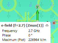
There are no articles to list here yet.